Related Products
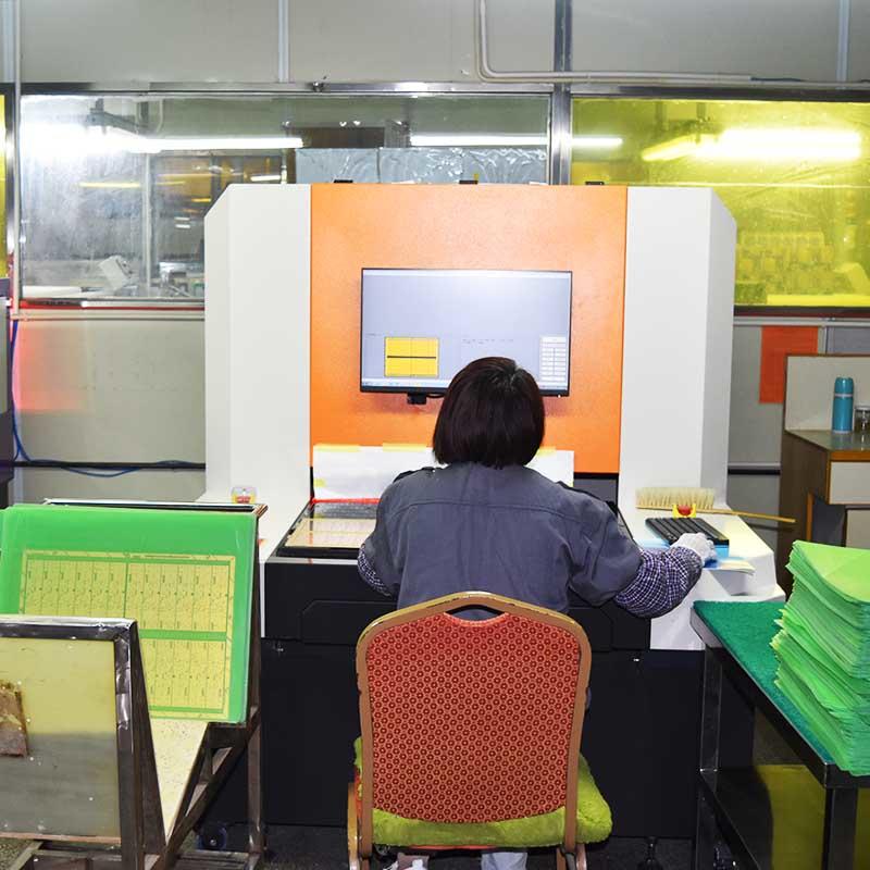
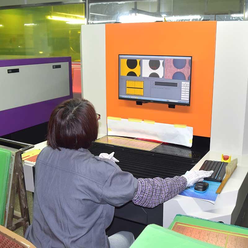
CNC PCB Machine Manufacturer
CNC PCB Machine Manufacturer


Product Information
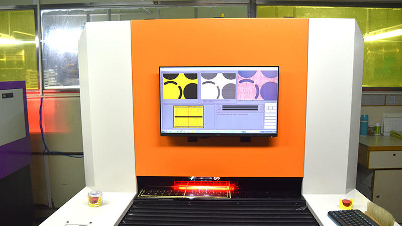
| AOI machine | ||
| NO. | Item | CKⅡ |
| 1 | Spindle No. | double spindle |
| 2 | Minimum line width/ line distance | 2.5 mil |
| 3 | Detectable line width range | 4/3/2 mil |
| 4 | maximum production | 470 sides (included 3 seconds per board time ) |
| 5 | Inspection size | 24″* 26″ |
| 6 | Inspection way | Morphological analysis based on CAM |
| 7 | Support CAM type | RS-274X;ODB++ |
| 8 | Alignment way | board side |
| 9 | Defect confirmation method | check up / Use inspection machine |
| 10 | Scanning light | LED cold light |
| 11 | Control system | Windows 64 bits |
| 12 | Size | 1980(D)*1600(W)*1750(H)mm |
| 13 | Weight | 1500KG |
| 14 | Power | AC 380V (3 phase 5 wire) |
| 15 | Air pressure | 2.5atm (30 psi) |
| 16 | Inspection material | copper/ gold board(include inner and outer side)/ soft board/ Dry film /Black Film |
| 17 | Checkable defect type | Short circuit/open circuit/Minimum line width/Minimum line spacing/gap/Copper deficiency/Convex copper/Copper slag/Pinhole/Porous/Missing hole/hole Blocking/hole Offset |
Product Description
▣ Novel structure and safety guarantee
▣ Quick program design and debugging integration,more convenient and quick operation;
▣ Automatic recognition of PCB surface and 180° reverse automatic identification system;
▣ Multi-program, multi-board test, making test more efficient and faster;
▣ Smart camera barcode recognition system (identifying 1D code and 2D code);
▣ Professional SPC analysis system to monitor and analyze product quality at all times;
▣ Multi-line monitoring system, all production line production status is clear
▣ Using remote programming and debugging control functions so that software control performance is stronger.
Logistics

We support both OEM & ODM packaging. Our normally delivery method are by the sea, by air, by international express (DHL, UPS, TNT, FedEx)
Copyright © 2021 Guangzhou Weyes Network Technology Co., Ltd. | All Rights Reserved

